Outline#
In this week’s lab you will:
- Get Digital set up on your personal device
- Build some simple circuits in Digital
- Learn the concept of abstraction, and apply it in Digital to build more complex circuits out of smaller circuits
- Understand what a multiplexer is, how it works, and build one in Digital
- Learn how to test a circuit in Digital
- Learn the basics of navigating the computer via the Linux terminal
- Install Git and learn to clone/push repositories
Introduction#
Welcome to the COMP2300/6300/ENGN2219 labs. These labs are the heart of the course, and they’re your opportunity to practice the core concepts you’ll need for the assignments. They are also your chance to explore and ask questions. If you don’t understand all of what’s going on in the labs, that’s Okay - for two reasons:
- You should use the lab sessions to ask as many questions as you want
- One of the best ways to learn is talking with other students
Today we aim to familiarize you with the variety of programs and systems you’ll use throughout the course. We will be using the Linux computer labs in the CSIT and Hanna Neumann (145) buildings. Unfortunately, computers outside of these labs won’t have the software required for working with the Digital simulator; thankfully, the CSIT building is open 24/7 and has plenty of free computers outside of class hours.
Often in labs, key information is highlighted in one of the following ways:
General notes, information, and references to documentation.
The actual tasks that you will be required to complete in a lab.
If there’s something difficult or a common pitfall that you may run into.
Sometimes you need to think about stuff before you go ahead. If you see something in a pink box, that’s your clue to pause and think—how do you expect the next part will work? Take a moment to think before you blaze away and start designing because then you can check whether you understand what’s going on or whether you’re just copy-pasting stuff without really understanding it. If you don’t understand it perfectly, that’s okay—ask your lab neighbor (or your tutor) to help you understand.
The lab sessions will have plenty of chances to discuss things with others in your lab group. Read the question and discuss it with your lab neighbor that sits near you. If you have a problem with your work, or if there’s something you don’t understand, the first thing you should do (after thinking about it) should be to ask another student. They might not know the answer straight away, but you might find that you can work it together.
All assessment submissions in this course happen through GitLab. It is a good habit to push your lab work to GitLab, especially as future labs will often depend on work in past labs. You’ll get accustomed to using Git before you really need to use it in your assignments. Having your work on GitLab also makes it really easy to show a tutor or your fellow classmates what you’ve done if you have further questions, as you can access all of your lab work on the GitLab website. We’ll add these push boxes as a friendly reminder to do so.
The material in these lab sessions will cover the concepts and knowledge you’ll need for your assessment items. However, sometimes there are interesting extension exercises you might try if you want to go deeper. If you don’t know how to approach the problems in the purple boxes, that’s okay - we don’t expect you to be able to complete these exercises, and you’ll do just fine in the course if you can do all the rest of the stuff in the labs. Still, it’s a chance to ask your lab mates and tutors and stretch yourself if you have time.
Exercise 1: Installing Course Software#
The first step is to set up the software we use in this course.
- If you are using a lab machine, then congratulations - most of the work has been done already!
- If you are working on your own computer, there are a few different things to install. You can continue reading the lab while the software installs itself. The instructions are on a separate page here.
Exercise 2: Using the Terminal#
We will first look at how to use the terminal to interact with the computer.
First, open a terminal. There are two sets of instructions - one for a lab machine, the other for your own device.
Lab Machine#
Like any other application, you can find it in the applications menu. Alternatively, press Ctrl + Alt + t.

Once open, you should see something like this:
uXXXXXXX@l115lt12:~$
This is the terminal prompt. It consists of your username (uXXXXXXX),
the computer you’re logged in to (l115lt12, the twelfth machine in N115, for this example)
and the directory your terminal is in (~), the home directory.
Your Own Computer#
The easiest way to open a terminal is through VS Code. As in the software install instructions, open VS Code. From the terminal menu at the top of your screen, open a new terminal. You should be greeted by some text similar to this:
username@computername:~$
This is the terminal prompt. It consists of your username,
the computer you’re logged in to and the directory your terminal is in (~), the home directory.
If you’ve installed Git on a Windows computer, you can also right-click inside the file explorer and select Git Bash Here. This will open a terminal that is in the directory open in the file explorer.
Terminal Exercises#
Regardless of whether you are using a Lab machine or your own device, the terminal commands should all look, and behave, the same way.
Try running the pwd command. You should see something like this:
uXXXXXXX@l115lt12:~$ pwd
/students/uXXXXXXX
uXXXXXXX@l115lt12:~$
What do you think the pwd command does?
The following table contains some commands you may find helpful throughout the course.
| Terminal Command | Name | Usage |
|---|---|---|
cd directory |
change directory | Changes the working directory to the directory given. |
cd ~ |
~ is an alias for your home directory. Will change to your home directory. |
|
cd .. |
Move up into the parent directory (if one exists). If you are in /students/uXXXXXXX/Desktop and you type cd .., you will end up in /students/uXXXXXXX
|
|
ls |
list | Lists the contents of the directory you are currently in. |
pwd |
print working directory | Shows the current working directory of the terminal. |
cat file |
Displays the contents of a file as text. | |
mkdir directory |
make directory | Makes a new directory with the given name. |
rm file |
remove | Deletes a file. Use with caution |
man command |
manual | Opens a manual page for the given command. Press f, b, q to scroll forwards, backwards, and exit the manual. |
This table is a very small selection of all of the available terminal commands. If you’d like to learn more, feel free to search the internet. There are many cheat-sheets for reference when using the terminal that are available online, such as this one.
You can paste to a terminal with Ctrl + Shift + v, or Right-Click and paste.
If you are typing in a command, try entering the first few characters, then press Tab - if possible, it will auto-complete what you are typing in. You can also look at what commands you’ve recently used in the terminal with the up and down arrow keys. Try running a command, then press the up arrow key.
If you’re completely lost you can watch a handy video we’ve made here.
Exercise 3: Git#
Now that your software is all ready to go, it’s time to get a copy of your lab and see if everything works. In this course, you’ll be using Git a lot, and you’ll have a lot of Git repositories (repos for short). Git is a distributed version control system. In plain English, it is a program that you can use to keep track of changes you make in a file, or collection of files (repository). Because Git is a distributed system, lots of people can work on the same thing concurrently and merge their changes later. For example, you may have a copy of an assignment repository on your laptop, the lab machines, and the CECS GitLab website at the same time. Since you can access the CECS GitLab server from any computer which has Git installed, it is a good idea to store your work there.
Git has a lot of features and tools, but in this course, there are only three that you will use frequently:
- Creating your fork and making a local copy of the repository (using fork and clone)
- Updating the local repository and synchronizing the content with GitLab (using pull)
- Committing your local changes and upload them to GitLab (using add, commit, and push)
Let’s begin.
- Log in with your uni ID/password and open the lab template on GitLab here.
- Fork the repository by clicking on the fork button. This will create your own copy of the lab repository.
- Pick your username as the namespace, and Private as the visibility. Leave the other settings untouched. Click “Fork Project” when done. The page will redirect you to your new fork when it is ready.
- Check the URL bar and make sure it contains your UID.
gitlab.cecs.anu.edu.au/YOUR_UID/comp2300-2024-lab-pack-1This means you are looking at your copy of the lab, and not the template. Once you’ve done this, click Code and copy the address next to “Clone with HTTPS”.
- Open a terminal and clone with the Git clone command:
git clone ADDRESS_FROM_STEP_4_HEREType in your UID and password when requested.
- You should now have a local copy of the repo on your computer. Try moving to the repo’s folder with the
cdandlscommands from earlier.
Congratulations! If you’ve got to this point unscathed, you’ve successfully forked, cloned, and pulled. You’ll revisit Git later when we cover the add, commit, and push part of using Git—after you’ve made some changes to your lab.
Take your time to familiarize yourself with Git early in the course—you won’t be able to submit the assessment items any other way. We also have videos about using Git on the course youtube channel.
Recommended only for lab machines: If you don’t want to type in your uid and password every time you pull and push, you can set up Secure Shell (SSH) keys that authenticate without the need for usernames and passwords. See this page for details. However, use of SSH keys requires either being on campus or connecting through the GlobalProtect VPN.
Interlude: Digital Electronics and Logic#
All real world circuits are analog, and have parameters like voltage and current that can be measured. These parameters are continuous, and can take on infinitely many values. In this course, we stay firmly within the realm of digital electronics and logic, where much of the ugliness of the real world is swept under the carpet, and we consider only two states that a point in a circuit can be in: LOW \((0)\) or HIGH \((1)\).
The actual voltage levels that these correspond to is arbitrary and for us not important. The important take away is that any sort of information (music, pictures, words) can be encoded as numbers, and those encoded still as sequences of LOW and HIGH electrical signals, or bits (binary digits). The sequence of words you are reading now, rendered through thousands of pixels on your screen, are at the end of the day nothing more than a collection of electrical impulses moving through a series of circuits that perform operations on them.
George Boole was the first to formalise a system of mathematics, called Boolean Algebra based on only two possible states, well before the existence of computers (Boole’s work predates the first transistor by just over a century). Unsurprisingly, much of the terminology in digital electronics is borrowed from Boolean algebra.
The names for the two states True (or HIGH, or \(1\)) and False (or LOW, or \(0\)) are largely arbitrary. You will need to be comfortable with switching between them.
Much like addition \(+\) and multiplication \(\times\) are operations in the algebra you learned in high school, Boole defined a series of operators for his system of mathematics, called Boolean operators.
The core boolean operators are:
- AND, (conjunction) notated as \(\land\)
- OR, (disjunction) notated as \(\lor\)
- NOT, (negation) notated as \(\lnot\)
The \(\land\) and \(\lor\) operators are binary operators. Here, binary refers not to boolean logic, but to the fact that they take two inputs (sources or source operands), and return one output (much like addition or multiplication do). Negation (\(\lnot\)) is a unary operator, meaning it takes in one input
- AND returns true if both inputs are true, and false otherwise.
- OR returns true if at least one input is true, and false otherwise.
- NOT returns true if the input is false, and false otherwise.
Truth Tables#
Some students may not have seen a truth table before in previous courses, and may be completing the lab before the lecture on this topic. That’s okay! Please ask a tutor or lab neighbour for help.
We can describe the function of these boolean operators using a truth table, by writing down the output for every combination of inputs.
\[\begin{array}{cc|c} A & B & A \land B \\ \hline 0 & 0 & 0 \\ 0 & 1 & 0 \\ 1 & 0 & 0 \\ 1 & 1 & 1 \end{array} \qquad \begin{array}{cc|c} A & B & A \lor B \\ \hline 0 & 0 & 0 \\ 0 & 1 & 1 \\ 1 & 0 & 1 \\ 1 & 1 & 1 \end{array} \qquad \begin{array}{c|c} A & \lnot A \\ \hline 0 & 1 \\ 1 & 0 \end{array}\]The logical operators themselves are also notated in many ways.
- A AND B is written as \(A \land B\), \(AB\) or
A & B. - A OR B is written as \(A \lor B\), \(A + B\) or
A | B. - NOT A is written as \(\lnot A\), \(\overline{A}\),
!A,~A,A'
Confusingly, \(+\) can also mean addition, so be careful!
The output of any combinational circuit (one where there are no feedback loops) depends entirely on what the inputs are set to. Since there are finitely many different combinations the inputs can be, we can describe the behaviour of a circuit by methodically listing the outputs for every combination of inputs in a table, much as we did to describe the behaviour of the logic gates above.
If a circuit had \(n\) different inputs, how many rows would the truth table have? What does this say about the suitability of describing a circuit using a truth table?
We can also simplify a truth table by using a reserved symbol \(X\), called a “don’t-care”. A row in a truth table should still be true regardless of the values chosen for the \(X\)’s.
What logic gate does the following truth table represent?
\[\begin{array}{cc|c} A & B & Q \\ \hline 0 & X & 0 \\ 1 & 0 & 0 \\ 1 & 1 & 1 \\ \end{array}\]Try to avoid using \(X\) for a boolean variable to avoid confusion.
From Logic/Maths to Gates#
In digital electronics, rather than working with components like resistors, inductors, capacitors and transistors, we deal with logic gates, or simply gates as our smallest atomic building block, and build all other components from gates. A logic gate is an idealized representation of a circuit that computes a boolean operation. Most of the time, we are not concerned with how a logic gate is physically realised, and will assume ideal behaviour (zero delay, infinite fanout, immunity to noise).
Later on in the course we may weaken these assumptions when discussing the layout of a computer to minimise signal propagation delay, and thereby maximise the speed at which the computer can run at.
Below are the 7 common logic gates you will encounter. AND, OR and NOT perform the same function as their boolean operation counterparts. XOR (eXclusive OR, pronounced “ex-or” or “zoar”) is a gate that returns true if the inputs are different. Equivalently, it returns true if exactly one of the two inputs is true (but not both).
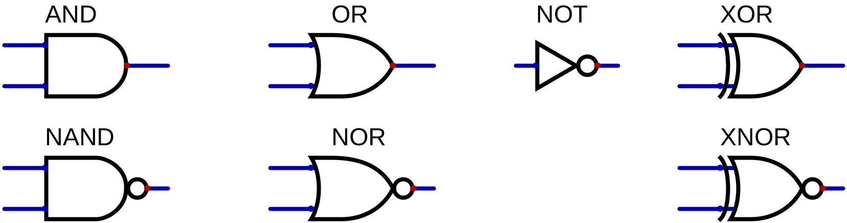
NAND, NOR, and XNOR (short for “NOT AND”, “NOT OR”, and “NOT XOR”) are negated versions of AND, OR, and XOR respectively. The bubble on the output represents that the output is negated (same as the bubble on the NOT gate).
There’s a gap in this diagram. Why haven’t we defined an NNOT gate?
The symbol for XOR in boolean algebra is \(\oplus\), with the corresponding truth table.
\[\begin{array}{cc|c} A & B & A \oplus B \\ \hline 0 & 0 & 0 \\ 0 & 1 & 1 \\ 1 & 0 & 1 \\ 1 & 1 & 0 \end{array}\]Exercise 4: Introduction to Digital#
Once the application opens, it should drop you directly into a tutorial (if not, go to the menu bar and navigate View -> Start Tutorial). This tutorial will step you through building your first circuit (a single XOR gate with 2 inputs and 1 output).
You may want to keep a copy of the Manual handy for reference. This is also available within Digital under Help -> Documentation. If you’re having trouble with the tutorial, page 6 of the manual provides a walk-through.
Digital Tips#
-
To move multiple components, click-and-drag a box around them, and then move as a group
-
To tidy a wire, click-and-drag a box around a bend in the wire. You can then move where the bend is to make things tidy.
-
While drawing a wire, you can click to pin the wire to the canvas, and add a bend in the wire at that point. Right-Click to stop drawing wire (Esc also works).
-
To delete a single wire segment, Ctrl + Left-Click on it, and then press Backspace or Delete.
Design Guidelines#
-
A circuit is cleaner if all the inputs are on the left/top, all the outputs are on the right/bottom, and the signals flow left-to-right/top-to-bottom. For this reason, Digital will place inputs facing right, and outputs facing left by default.
-
Wires should usually be either horizontal or vertical, and meet at right angles. Exceptions are often made for sequential circuits (where the output flows back into the inputs), or for parallel wires that need to swap places. If you’d like to draw a diagonal line, press d to toggle between diagonal mode while drawing a wire.
-
A list of keyboard shortcuts can be found in Section A.9 of the manual.
-
None of these guidelines are hard rules. If your circuit is otherwise simpler or improved by violating one of these guidelines, then do it.
For more like this, take a look at our Digital Style Guide and Tips & Tricks pages.
Exercise 5: Multiplexers#
We will be building a 2:1 multiplexer, a combinational circuit used to select one output from 2 or more inputs. Multiplexers are very useful components used to choose which signal to route to a bus, and we will be using multiplexers throughout the semester to build the CPU.
The standard symbol uses to notate a multiplexer is shown. It has two data inputs, \(A\) and \(B\), and a control input \(S\), that Selects which input is routed to the output called \(Q\).
- If \(S\) is \(0\), then \(A\) is copied to \(Q\).
- If \(S\) is \(1\), then \(B\) is copied to \(Q\).
The multiplexer can be thought of as akin to a controlled switch that selects between one of two inputs.

Using don’t cares (\(X\)), try to rewrite the above truth table using as few rows as possible.
Sum of Products#
Now that we have a truth table for the multiplexer, we can convert it to a boolean equation that describes the behaviour of this circuit. One technique for this is called “sum of products”, where for each row of the truth table where the output is \(1\), we AND together all the variables in that row. This is called a product (as AND is often notated by writing the variables next to each other, \(A \land B = AB\), like a product). The “products” are then all combined with logical OR to make an expression (as the output is true if any one of the rows is satisfied). This is called a sum (as OR is notated using plus, \(A \lor B = A+B\)).
For example, given the truth table for the XOR gate from before, we can write the boolean equation as \((A \land \lnot B) \lor (\lnot A \land B)\), or more compactly as \(A \overline{B} + \overline{A} B\), from which the origin of the term “sum of products” now becomes apparent.
Using the techniques described above, design a boolean equation for \(Q\) in terms of \(A\), \(B\), and \(S\).
The “sum of product” technique always works, but it seldom gives you the best (shortest) answer. Can you come up with an even shorter boolean equation for the above truth table?
Open the lab file 2_to_1_mux.dig in Digital. Using this file as a template, construct a logical circuit that implements the behaviour of a multiplexer using logic gates. Obviously, don’t use the pre-built multiplexer component!
Testing the Multiplexer#
Occasionally, a poorly written test can cause Digital to crash. You should always save your work before writing or running a new test.
We can also test our circuits. Add the component Misc. -> Test case. Place it somewhere on the canvas.
Right-click on the test case, and click Edit. This will open an editor in which you can write your test case. You might want to have a read through the Help section to see how to write more advanced tests, but for the moment we will just write out a full truth table.

Using your truth table from before, write a test for the multiplexer, using the same labels for inputs/outputs that you used for the multiplexer (use X as the “don’t care” symbol).
For example, if we were testing an AND gate with inputs A and B, and output Q, the test case would be formatted as follows.
A B Q
0 0 0
0 1 0
1 0 0
1 1 1
Run the test and verify that for every combination of inputs, the expected output matches the behaviour of the circuit. (Included in the below image is the example test case for if we were testing an AND gate).

Testing custom components is vital, as we wouldn’t want to build anything bigger using the multiplexer before we trust that the multiplexer works correctly.
Exercise 6: Pushing Your Work Back to GitLab#
Now you’ve made changes to your repository, don’t forget to commit & push to GitLab! If you don’t push, then your new commits won’t be uploaded to the GitLab server. The labs aren’t worth any marks, but this is good practice for when you’re trying to submit an assignment, as we mark what is on GitLab. It also means you’ve got a backup of your lab material in case something goes wrong.
Now you’ve done some work, it’s time to complete the second half of our Git workflow. Let’s begin:
- Open a terminal and navigate to your Git repo’s folder. (
cdandlsmay be useful for this) - Add all of your changes to a new Git commit with
git add -A - Optionally verify that everything has been added with
git statusIt should show a list of changes that have been prepared for the commit. On your terminal the added modified files would appear in green text. For example,
On branch master Your branch is up to date with 'origin/master'. Changes to be committed: (use "git restore --staged <file>..." to unstage) modified: 2_to_1_mux.dig - If this is the first time you’ve used Git, run the following commands one at a time with your name and email inserted.
git config --global user.name "John Smith" git config --global user.email "u1234567@anu.edu.au" - Finish your new commit and give it a message like this:
git commit -m "Survived lab 1!" - Make sure your work ends up on the CECS GitLab server by pushing:
git push
Congratulations! If you’ve got to this point unscathed, you’ve successfully added, committed, and pushed. Have a look on GitLab and see if you can find the repository you’ve just pushed. Whenever you see an orange push box in a lab, or when you’ve done some work on an assignment, just repeat the steps above.
This is also a good point to talk about CI as you may be receiving an email soon about the pipeline failing. CI is something we will be using a lot in the course so its good for you to understand it, but the even better news is that its all done for you, nothing more to set up woohoo!
Okay well maybe I lied a little, it’s good for you to understand what is going on, and to turn off those email alerts if they annoy you. You can read more about CI here.
Can you keep your labs or assignments shared and up to date between the lab computers and your own device with Git?
Wire Splitter#
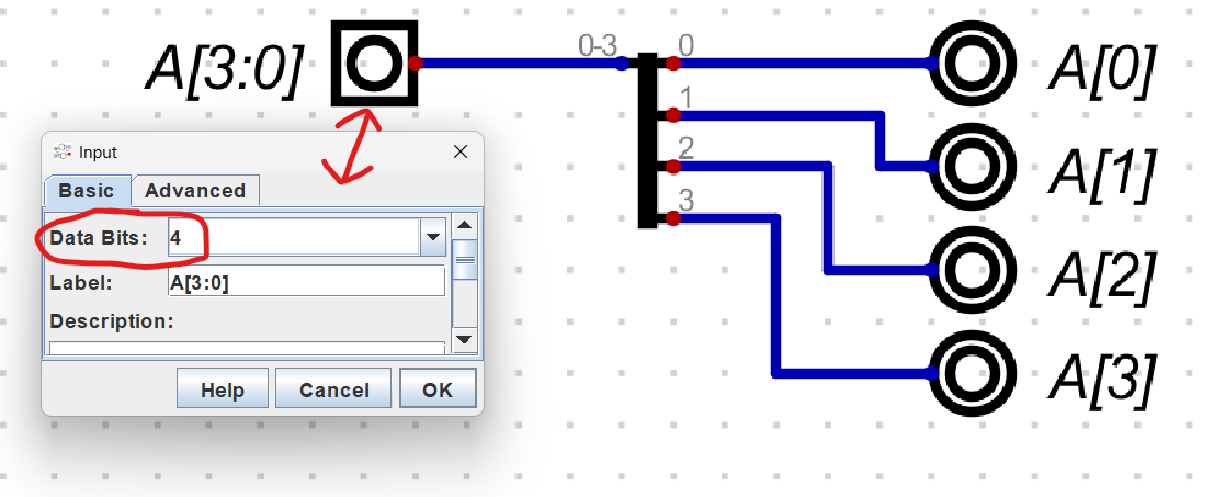
The computer we will eventually build during this semester is a 16-bit machine. You might notice that in real life, a wire can only send a signal of 0 or 1 (either current is flowing or it’s not). To send more than 1 bit of information, you would need multiple wires to send several signals. A 16-bit machine is one which uses numbers that are up to 16 binary digits, which requires 16 wires to send. However, drawing 16 individual wires back and forth is tedious and error-prone.
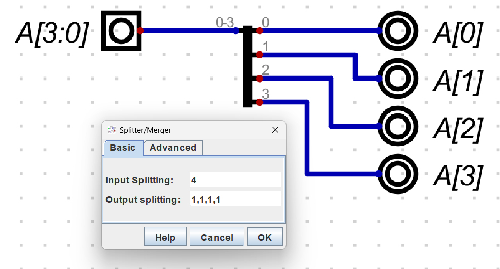
Thankfully Digital abstracts some of this away by allowing inputs and outputs to represent a collection of binary values rather than a single bit. Often, we will need to separate this bundle of wires to extract out particular bits of interest. This is where the wire splitter comes in handy.

In the example above, the wire on the left side of the splitter is 4 bits (can be considered as a bundle of 4 wires), which we split using the splitter into 4 wires each carrying 1 bit. In the simulation, the input is 4 bits and is set to 7. In binary, 7 is written as 0111, and you can indeed see on the right side of the splitter that the lights that are on match the bits that are 1 in 0111 reading from right to left.
Notice that the lowest index on the splitter, \(0\), represents the rightmost/least significant bit of the input. Indexing the bits of a number this way is a convention called little endian.
Given that we tend to read numbers from left to right, what benefit is there to indexing from right to left? Hint: recall how in decimal, each digit corresponds to a multiple of something, e.g. you have a ones place, a tens place, a hundreds place, and so on. In binary, it’s the same except with powers of 2. Can you see a connection between each bit’s “place” and the little endian index it would have?
The opposite convention (indexing bits from left to right) is called big endian.
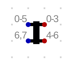
The wire splitter component (Wires -> Splitter/Merger) is a device that can be used to split a wire bundle into smaller bundles, or combine smaller bundles into bigger bundles.
Given a bundle with \(n\) wires, each wire has an index, wire \(0\), wire \(1\), … wire \(n-1\).
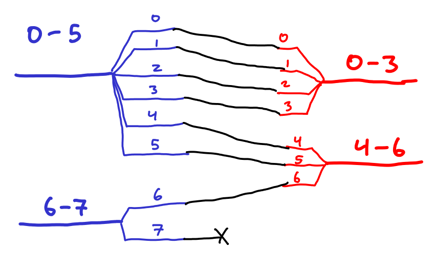
Click on the Help button for the wire splitter to see a description of how to use it. In summary, you can write a set of numbers separated by commas, and the wire-splitter will choose to bundle the wires together in sizes given by the numbers, from the 0th wire onwards.
For example, if the input splitting is 6,2 and the output splitting is 4,3, then the splitter would be internally wired up like so:
So far, our examples have simply stated the number of wires desired for each input and output. To specify a specific range of bits, range notation is used. Eg: 0-3 will create an input or output with bits 0, 1, 2, and 3. 5-5 will create an input or output with just bit 5.
You will also need to change the bit counts of the components that you connect to a wire splitter. For example, in the example above, we set the input to a 4-bit one by right clicking on it as shown below.
Constant Value#
The constant value component Wires -> Constant Value can be used when you need to route a fixed value into part of a circuit. Both the number of bits and the value can be adjusted.
Exercise 7: Building a Shifter#
Open shift.dig as a template. There is a 8-bit input A and 8-bit output B. Build a circuit that performs a logical shift left, that is, if we denote bit i in A as A[i], and bit i in B as B[i], then the behaviour of the circuit should be
B[7] = A[6]
B[6] = A[5]
B[5] = A[4]
B[4] = A[3]
B[3] = A[2]
B[2] = A[1]
B[1] = A[0]
B[0] = 0
This operation would be denoted as B = A << 1. “<<” is called the left shift operator, and here we are shifting
everything left by 1 bit, hence A << 1. So for instance, if A = 00011101 in binary, B = 00011101 << 1 = 00111010; all the
bits are shifted left by 1.
Your circuit should be made only of constant values and wire splitters (don’t just use a pre-built shifting component!)
Complex Testing#
We’d now like to test our shifter, but it would be very tedious to write out a truth table with 256 entries. Thankfully, Digital provides a mechanism for which we can describe the behaviour of a circuit as an expression, and then test that expression against the behaviour of the circuit for all possible combinations of inputs.
For example, we can use the loop(i, k) ... end loop construct to create a loop, where i runs through all values \(0 \leq i < k\), and test that B is always equal to A << 1, regardless of the value of A.
    A    B
loop(i, 256)
    (i)  (i<<1)
end loop
Since A is a 8-bit value, we need to try all values for i between 0 and 255. Doing so autogenerates the test cases as if we had tediously written the 256 lines of the table by hand where (i) is for the A column, and (i<<1) is for the B column.
These full tests that cover all possible input configurations are only possible for relatively simple circuits, as given \(n\) input bits there is a total of \(2^n\) possible configurations to test. Anything more than \(n=20\) or so is intractable to test. For very large circuits, we can still cover a subset of the inputs by randomly generating test cases, though this doesn’t guarantee that all errors have been found.
We can use the random(n) function, which generates a random number \(r\) in the range \(0 \leq r < n\), and the let keyword, to assign a temporary variable to that randomly generated value.
For example, supposing we had a circuit that adds 16-bit numbers, and we wanted to test 100 random 16-bit numbers, we could write
    A   B
loop(i, 100)
    let y = random(1<<16);
    (y) (y<<1)
end loop
What is the significance of 1<<16 in this expression? Why is this equivalent to \(2^{16}\)?
As shown in the Help section for writing complex test cases, the general structure for writing complex test cases is:
    var1 var2 ... varn

code to define how to autofill each row such as loop or while

    (var1 value) (var2 value) ... (varn value)

code to stop the autofill such as end loop or end while, or more code to define how to autofill each row
Add an appropriate test to shift.dig to verify that the circuit compute the output B as A << 1 (the logical left shift of A by one bit) for all possible inputs.
Exercise 8: Abstraction I#
Once we have made a circuit out of gates, we can treat the entire circuit as if it is a single component, from which we can build bigger components. This concept of abstraction is something that will be integral throughout the semester to building a CPU, as it would be too complex to talk about the operation of a computer on the logic gate level. The abstracted building blocks we will see (multiplexers, adders, registers, etc). along the way are themselves built out of other abstracted components. Logic gates themselves are also an abstraction, being built out of some kind of real world analog switching element (MOSFETs, transistors, etc). that for convenience we treat as an idealised digital component.
We will be using the multiplexer we built in 2_to_1_mux.dig to build a larger family of multiplexers that operate on wider data inputs, or more inputs, (or both!)
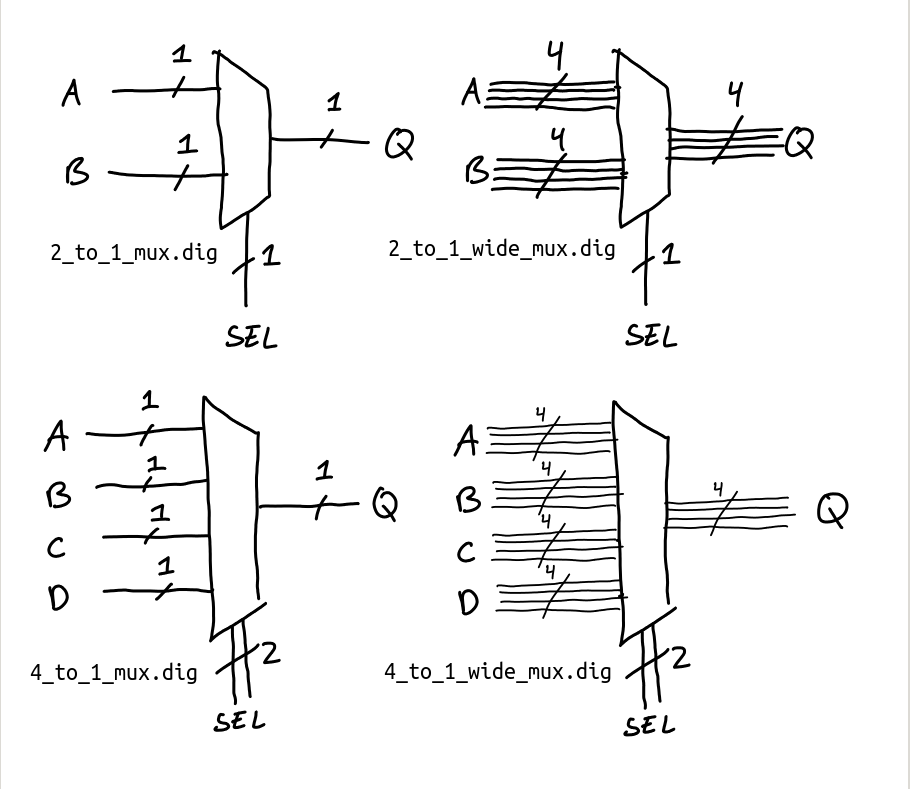
We would like to use the multiplexer we just created to build a bigger circuit, one that chooses between two 4-bit signals A and B using a 1-bit select line SEL, copying the chosen signal to the output Q.
Open 2_to_1_wide_mux.dig as a template. Under Custom -> 2_to_1_mux you will find a component representing the multiplexer we built earlier.
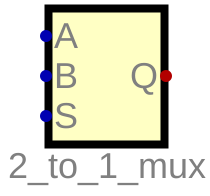
The pins on our custom component are labelled with the same labels we chose for the inputs/outputs. The inputs are denoted with blue pins, the outputs with red pins. Use copies of 2_to_1_mux together with wire splitters to build a 4-bit 2-to-1 mux that satisfies this description above.
You can consider each input pair of bits (A[i], B[i]) once you’ve used a splitter to isolate them. Compute the result for each bit, and combine back together.
As before, write a test case that validates the correctness of 2_to_1_wide_mux.dig for all possible inputs. (There should be \(2^9\) combinations, the 4 bits for A, the 4 bits for B and the 1 bit for S). If you get stuck, ask a tutor.
Exercise 9: Abstraction II#
Complete and test 4_to_1_mux.dig. This multiplexer has a select line with two bits, and chooses between one of four one-bit inputs. The behaviour is described here as a Digital test case. As you may have used it already, you should see that X is here to represent “don’t care” (in that the value of X is irrelevant, and the row in the truth table would still hold regardless if any/all of the X were replaced with any value).
A B C D S     Q
0 X X X 0b00  0
1 X X X 0b00  1
X 0 X X 0b01  0
X 1 X X 0b01  1
X X 0 X 0b10  0
X X 1 X 0b10  1
X X X 0 0b11  0
X X X 1 0b11  1
Again, using 2_to_1_mux, build a 4-to-1 multiplexer satisfying this property. Don’t forget to test it!
Exercise 10: Abstraction III#
Finally, complete and test 4_to_1_wide_mux.dig. Using any of the multiplexers you’ve already built, build a version of 4_to_1_mux that selects one of 4 inputs to an output, and the inputs/outputs are 4 bits wide. The select line is still 2 bits wide. There’s quite a lot of combinations of inputs here, so instead of an exhaustive test, test 1000 randomly generated inputs, for each of the possible select inputs: 00, 01, 10, and 11.
Imagine if we had asked you to complete the 4_to_1_wide_mux.dig from the logic gate level. Hopefully this emphasises the importance of abstraction!
Conclusion#
You’ve probably seen enough of multiplexers for a lifetime now. Of course, Digital has a built in multiplexer (Plexers -> Multiplexer). By placing this multiplexer and right clicking on it, we can change attributes like the data width of the inputs, and the number of selector bits (which dictates how many inputs the multiplexer can switch between). However, the key takeaway from this lab is that you can build big complex circuits from smaller simpler circuits. This concept is called abstraction and this a key concept for the rest of the semester.
Curiously, multiplexers can also be used as a lookup table to emulate any other gate. Open mux_emulate_xor.dig as a template. There is a test already existing that verifies that Q = A XOR B. Using only wire splitters, constant values, and the 4_to_1_mux.dig components, build a circuit that passes this test.
Resources#
Labs may have a resources section with links to relevant material. We also have a resources page on the website covering course related resources and suggested further reading.